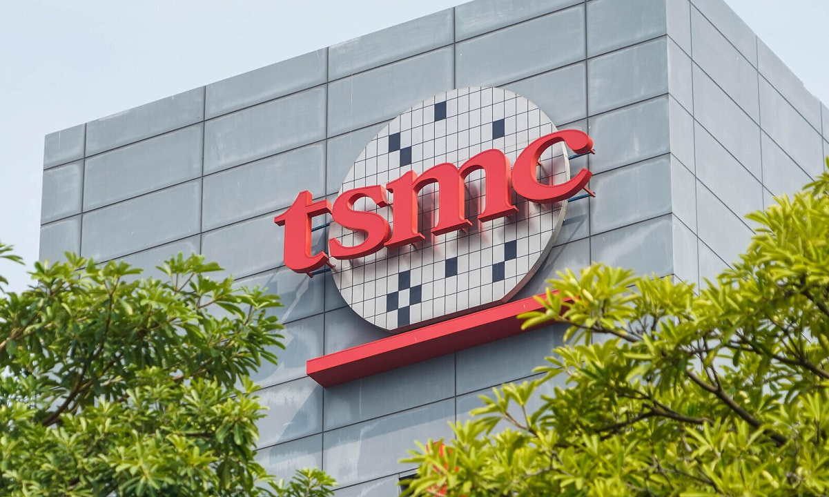
TSMC plans to build its third plant in Arizona

ARIZONA – TSMC has announced plans to build a third fab in Arizona, leveraging the most advanced semiconductor process technology in the United States.
Together with the U.S. Department of Commerce, the company has signed preliminary terms for direct funding of up to US$6.6 billion under the CHIPS and Science Act.
As the company moves forward with the completion of its first fab, and in February 2024 celebrated the placement of the final steel beam of its second fab, the third plant brings TSMC’s total investment to more than US$65 billion, making the Phoenix plant the largest foreign direct investment in Arizona history and the largest foreign direct investment in a greenfield project in U.S. history.
The three TSMC Arizona fabs are expected to create 6,000 direct high-tech, high-wage jobs, creating a workforce that will help support a vibrant and competitive global semiconductor ecosystem that enables leading U.S. companies to access cutting-edge, domestically manufactured semiconductor products along with a world-class semiconductor foundry.
“With this vital investment made possible by the CHIPS Act, this partnership will continue to thrive. We are at the forefront of our nation’s economic future because of our highly skilled workforce and dynamic economic engine, and TSMC’s growth and investment right here in Arizona will continue to demonstrate to the world that our state is the best place for businesses to invest,” said Governor Katie Hobbs.
“The CHIPS and Science Act provides TSMC the opportunity to make this unprecedented investment and provide our foundry with the service of the most advanced manufacturing technologies in America,” said TSMC President Dr. Mark Liu.
“They are the innovators driving demand for the most advanced silicon TSMC has to offer. As their foundry partner, we will help them unleash their innovations by increasing state-of-the-art capabilities through TSMC Arizona. We are delighted with the progress of our Arizona plant to date and are committed to its long-term success,” said TSMC CEO Dr. C.C. Wei.
The first TSMC Arizona fab is on track to begin production leveraging 4nm technology in the first half of 2025. The second fab will produce the world’s most advanced 2nm process technology with next-generation nanosheet transistors in addition to the previously announced 3nm technology, with production to begin in 2028. The third fab will produce chips with 2nm or more advanced processes, and production will begin by the end of the decade. Each of the three fabs, like all of TSMC’s advanced fabs, will have a cleanroom area roughly twice the size of an industry-standard logic fab.
In addition to the proposed $6.6 billion in direct funding, the PMT also proposes to provide TSMC with up to US$5 billion in loans. TSMC plans to apply for investment tax credits from the U.S. Treasury Department of up to 25% of qualified capital expenditures at TSMC Arizona. The company remains committed to its long-term financial targets, which are a compound annual growth rate (CAGR) of 15-20% revenue in USD terms, gross margin of 53% and above, and return on equity (ROE) of 25% and above.
